Metamateriały elektromagnetyczne (EM) to syntetyczne struktury o specjalnych właściwościach elektromagnetycznych, takich jak ujemna wartość współczynnika załamania światła – postulowana przez Veselago [1]. Stały się aktywnym obszarem badawczym, ponieważ wykazują niezwykłe reakcje EM nieosiągalne dla materiałów naturalnych. Niektóre atrakcyjne przykłady zastosowań to supersoczewkowanie, maskowanie, sztuczne przewodnictwo magnetyczne i bardziej ogólnie projektowanie materiałów do transformacji współrzędnych [2,3]. Jednym ze sposobów realizacji takich funkcjonalności są okresowe lub półokresowe układy struktur rezonansowych, takie jak rezonatory z rozszczepionym pierścieniem (SRR) [4]. Drugim sposobem realizacji takich funkcjonalności była pełna trójwymiarowa struktura dielektryczna oparta na okresowej komórce elementarnej 3D []. Aby zrealizować modelowanie tych struktur, zastosowano model oparty na obwodach (rozproszonych) i pełny model symulacji EM.
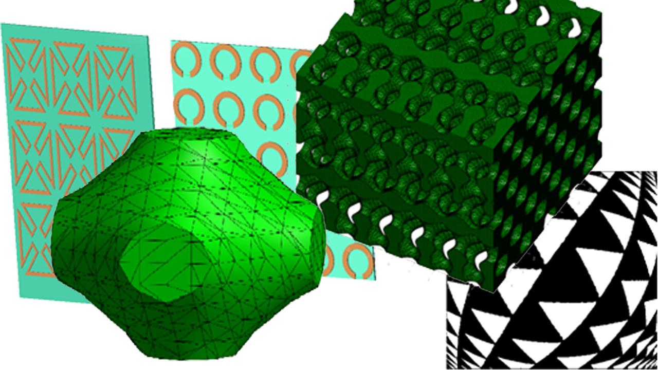
In case of metasurface (fig 1. A) most interesting phenomena are associated with a network of resonators (SRR). Based on this fact modeling of this structures takes account model of single SRR, and model of couplings in rezonator network. These models can be based on full Electromagnetic field simulation and (distributed) circuit model.
This is a first direction of research: method for effective modeling of metasurface. Further research directions are connected with metamaterials applications: for medical diagnostic (e.g. MRI lens), telecommunication (Artifical Magnetic Conductor - AMC, Electromagnetic Band Gap EBG and other) and biosensors in THz gap.
Dielectric 3D metastructures are a separate research direction. In this case, the key issues are: application of transformation optics methods for numerical EM field shaping, generating periodic 3D structures, full Electromagnetic field simulation and preparing 3D models (by 3D printer).
In fact, research are included: circuit theory, description of the behavior of the electromagnetic field in various materials, EM full field simulation, transformation optics, optimization methods, 3D printing problems and others.
At the Institute of Electronics, we conduct research on modeling the metasurfaces for : magnetic resonance imaging (magnetic lens), Artifical Magnetic Conductors - AMC and Electromagnetic Band Gap EBG for telecommunication application, for example in BAN network (Body Area Network), finally also for metasurfaces designed for THz Gap.
At present, our priority is that the acquired competencies in building and applying metasurfaces for given applications (medical, telecommunication and others).
- Prof. Sławomir Hausman, e-mail: slawomir.hausman@p.lodz.pl
- Dr. Łukasz Jopek, e-mail: lukasz.jopek@p.lodz.pl